

-
×
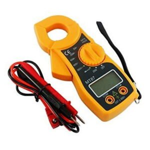 MT87 Mini Clamp Digital Multimeter AC/DC
1 × ₨ 1,299
MT87 Mini Clamp Digital Multimeter AC/DC
1 × ₨ 1,299
Subtotal: ₨ 1,299
₨ 47
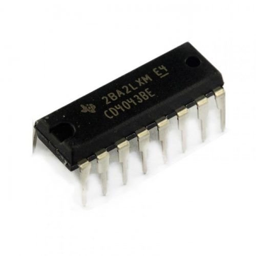
CD4043 Quad NOR R-S Latch Tri-state is a combinational logic circuit, that has two inputs S and R, and two outputs Q and Q. The state of this latch is determined by the condition of output Q. If output Q is 1 (High) the latch is said to be SET and if Q is 0 (Low) the latch is said to be RESET. An SR Latch or Flip flop can be designed either by two cross-coupled NAND gates or two-cross coupled NOR gates.
| Pin No | Pin Name | Description |
|---|---|---|
| 1 | Q4 | output of latch 4 |
| 2 | Q1 | output of latch 1 |
| 3 | R1 | reset input latch 1 |
| 4 | S1 | set input latch 1 |
| 5 | ENB | enable pin |
| 6 | S2 | set input latch 2 |
| 7 | R2 | reset input latch 2 |
| 8 | VSS | source supply |
| 9 | Q2 | output of latch 2 |
| 10 | Q3 | output of latch 3 |
| 11 | R3 | reset input latch 3 |
| 12 | S3 | set input latch 3 |
| 13 | NC | no connection |
| 14 | S4 | set input latch 4 |
| 15 | R4 | reset input latch 4 |
| 16 | VDD | Drain supply |
You can download the datasheet for CD4043 Quad NOR R-S Latch with Tristate
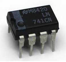
The LM741 series are general-purpose operational amplifiers which feature improved performance over industry.The amplifiers offer many features : overload protection on the input and output, no latch-up when the common-mode range is exceeded, as well as freedom from oscillations. The LM741C is identical to the LM741 and LM741A except that the LM741C has their performance ensured over a 0C to +70C temperature range, instead of 55C to +125C.
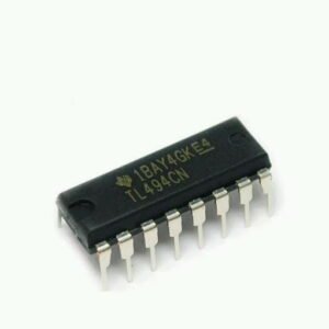
The TL494 device incorporates all the functions required in the construction of a pulse-width-modulation (PWM) control circuit on a single chip. Designed primarily for power-supply control, this device offers the flexibility to tailor the power-supply control circuitry to a specific application. The TL494 device contains two error amplifiers, an on-chip adjustable oscillator, a dead-time control (DTC) comparator, a pulse-steering control flip-flop, a 5-V, 5%-precision regulator, and output-control circuits.The TL494C device is characterized for operation from 0C to 70C. The TL494I device is characterized for operation from 40C to 85C.

There are no reviews yet.