

-
×
 5X Magnification Magnifying Glass with Illuminant
1 × ₨ 249
5X Magnification Magnifying Glass with Illuminant
1 × ₨ 249 -
×
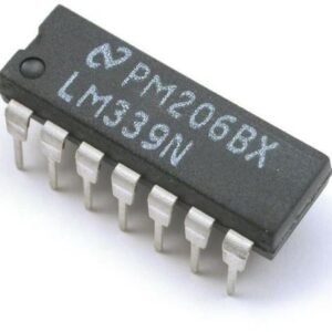 LM339 VOLTAGE COMPARATOR IC
1 × ₨ 55
LM339 VOLTAGE COMPARATOR IC
1 × ₨ 55
Subtotal: ₨ 304
₨ 36
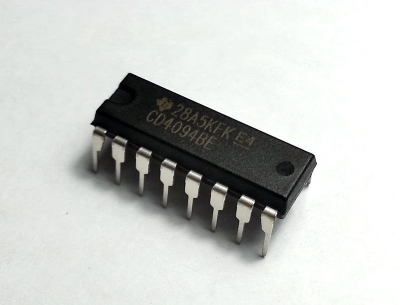
CD4094 Shift Register having a storage latch associated with each stage for strobing data from the serial input to parallel buffered 3-state outputs. The parallel outputs may be connected directly to common bus lines. Data is shifted on positive clock transitions. The data in each shift register stage is transferred to the storage register when the STROBE input is high. Data in the storage register appears at the outputs whenever the OUTPUT-ENABLE signal is high.
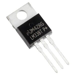
LM338T 5A Adjustable Voltage Regulator LM-338T is adjustable 3-terminal positive voltage regulators is capable of supplying in excess of 5 A over a 1.2-V to 32-V output range. They are exceptionally easy to use and require only 2 resistors to set the output voltage.
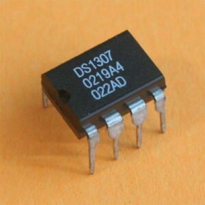
The DS1307 serial real-time clock (RTC) is a lowpower, full binary-coded decimal (BCD) clock/calendar plus 56 bytes of NV SRAM. Address and data are transferred serially through an I2C, bidirectional bus. The clock/calendar provides seconds, minutes, hours, day, date, month, and year information. The end of the month date is automatically adjusted for months with fewer than 31 days, including corrections for leap year. The clock operates in either the 24-hour or 12-hour format with AM/PM indicator. The DS1307 has a built-in power-sense circuit that detects power failures and automatically switches to the backup supply. Timekeeping operation continues while the part operates from the backup supply.

There are no reviews yet.