

-
×
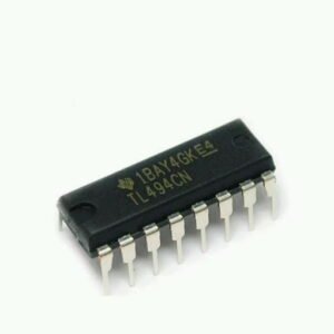 TL494 Current-Mode PWM Controller
1 × ₨ 62
TL494 Current-Mode PWM Controller
1 × ₨ 62
Subtotal: ₨ 62
₨ 36
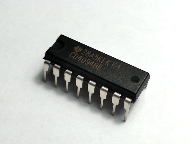
CD4094 Shift Register having a storage latch associated with each stage for strobing data from the serial input to parallel buffered 3-state outputs. The parallel outputs may be connected directly to common bus lines. Data is shifted on positive clock transitions. The data in each shift register stage is transferred to the storage register when the STROBE input is high. Data in the storage register appears at the outputs whenever the OUTPUT-ENABLE signal is high.
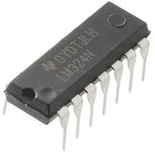
LM324 Operational Amplifier IC LM-324 consist of four independent high-gain frequency-compensated operational amplifiers that are designed specifically to operate from a single supply or split supply over a wide range of voltages. Wide Supply Ranges Single Supply: 3 V to 32 V (26 V for LM2902) Dual Supplies: 1.5 V to 16 V (13 V for LM2902) Low Supply-Current Drain.
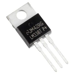
LM338T 5A Adjustable Voltage Regulator LM-338T is adjustable 3-terminal positive voltage regulators is capable of supplying in excess of 5 A over a 1.2-V to 32-V output range. They are exceptionally easy to use and require only 2 resistors to set the output voltage.
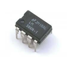
LM386 is a widely used audio amplifier IC manufactured in 8 pin dip, VSSOP, SOIC and other packages. The IC is basically designed for low voltage commercial applications, apart from commercial applications it is also a famous IC among electronic hobbyists and experimenters. The internal gain of the IC is set to 20 but it can be adjusted by connecting a resistor and a capacitor in series between the pin number 1 and 8, by this procedure the user can adjust the gain between 20 to 200. Due to the small size, low quiescent current and low voltage requirements this IC is ideal to use in wide variety of portable battery operated applications and devices.
There are no reviews yet.